
Semiconductor & Microelectronics
Precision at the Micro Level
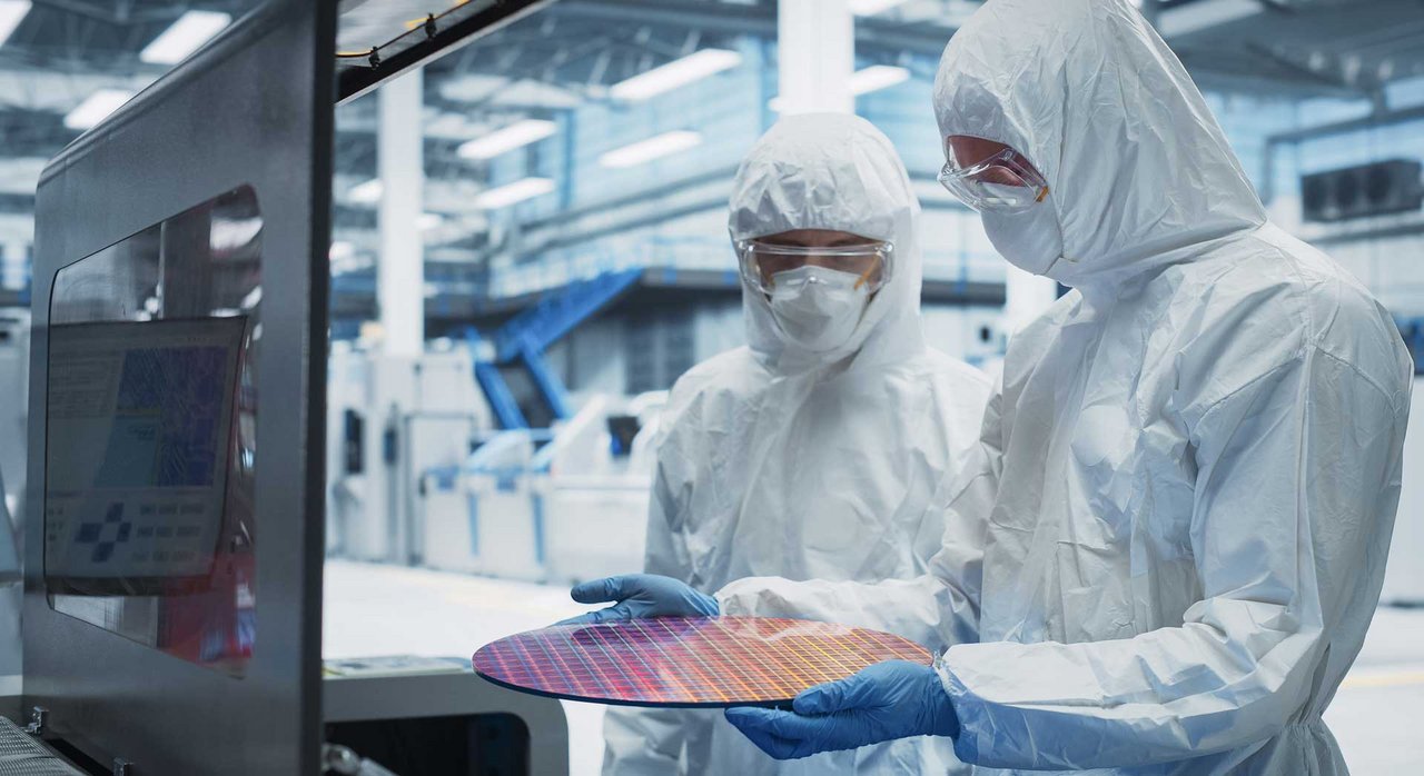
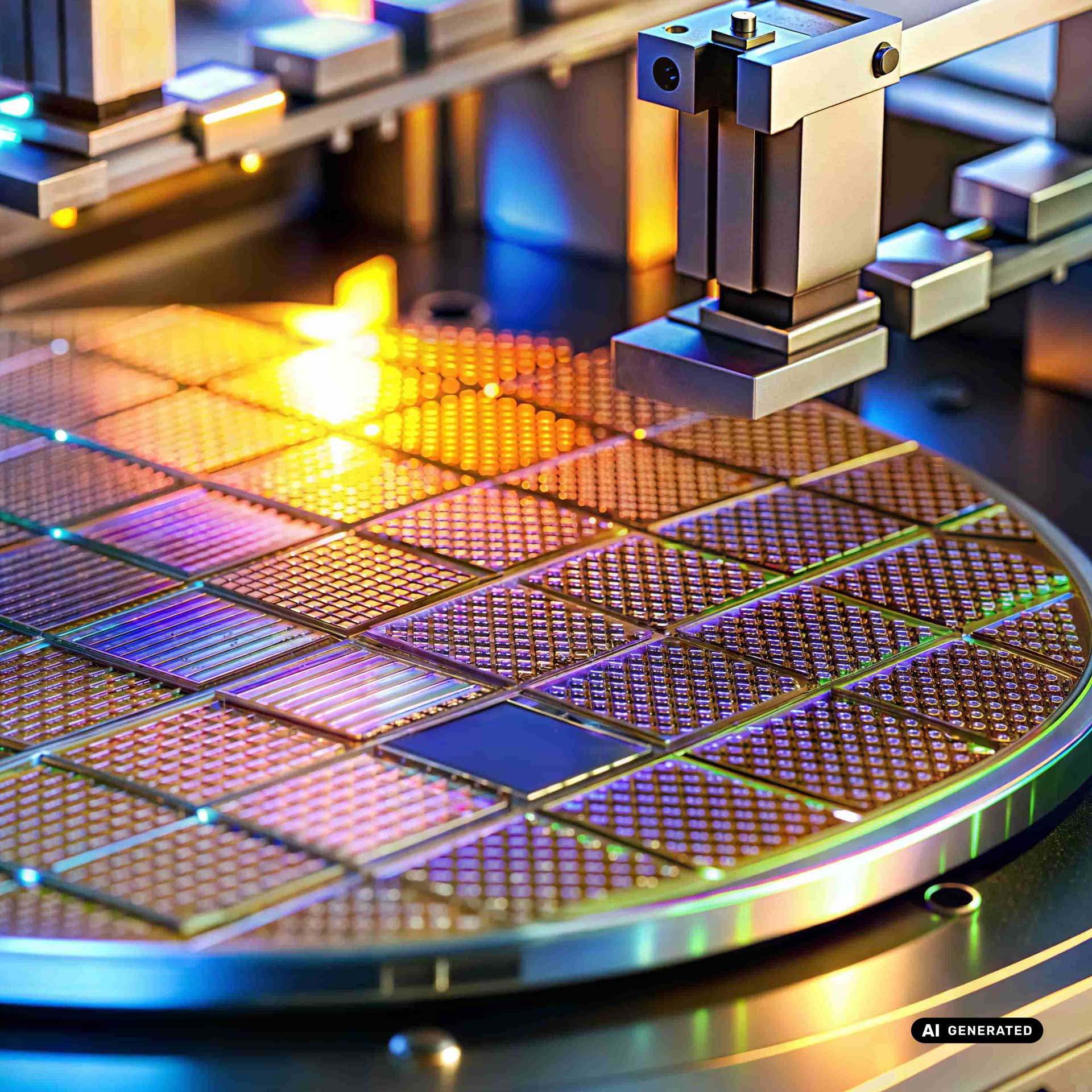
The semiconductor and electronics industry rely on advanced inspection technologies to ensure the highest standards of quality, reliability, and performance. From wafer fabrication to advanced packaging, precise inspection is essential to detect defects such as cracks, voids, contamination, and misalignment at an early stage. This includes wafer and die level inspection as well as the analysis of interconnects like microvias, and TSVs, enabling manufacturers to optimize yield and maintain process stability in increasingly complex production environments.
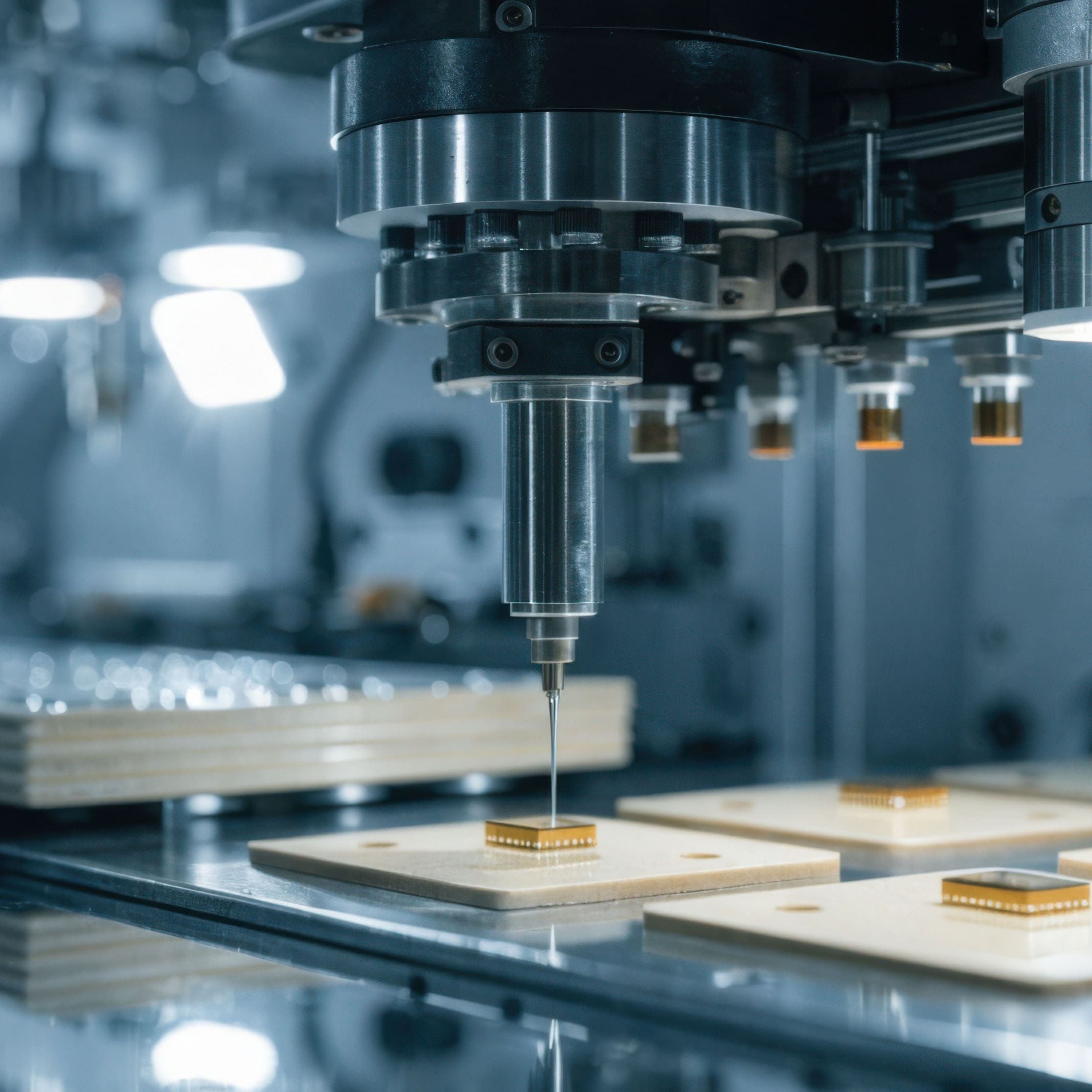
With the rapid evolution of advanced packaging, inspection plays a critical role in ensuring the integrity of solder balls, bumps, pads, and various bonding technologies such as wire bonding, flip-chip, hybrid, and direct bonding. In addition, 3D inspection of internal package structures and wafer-level process monitoring are key to guaranteeing performance and long-term reliability in high-density and high-performance applications.
In power electronics and advanced material processing, inspection is equally vital to ensure durability and efficiency. This includes the evaluation of DCB, AMB, and ceramic substrates, as well as sintered and soldered interfaces and bond integrity within power modules. Furthermore, Viscom’s inspection solutions enable precise analysis of advanced materials such as sinter, gold, and silver pastes, supporting accurate volume control, homogeneity, and stable manufacturing processes across a wide range of industrial application.

Why choose Viscom?
We make technology safe, reliable and sustainable!
40 Years of Expertise
Four decades of inspection know-how, combining deep industry knowledge with proven innovation to deliver trusted inspection solutions.
100% Defect Detection
Always advancing with the latest inspection solutions to achieve the highest detection rates and support zero-defect manufacturing.
Award-Winning Inspection Solutions
Industry-leading inspection systems recognized worldwide for outstanding performance, precision, and reliability across every production stage.
Contact
FIND THE RIGHT INSPECTION SOLUTION FOR YOUR Manufacturing process
Benefit from Viscom's award-winning inspection technologies and our global support from experts.
Applications
BGA / QFN Inspection
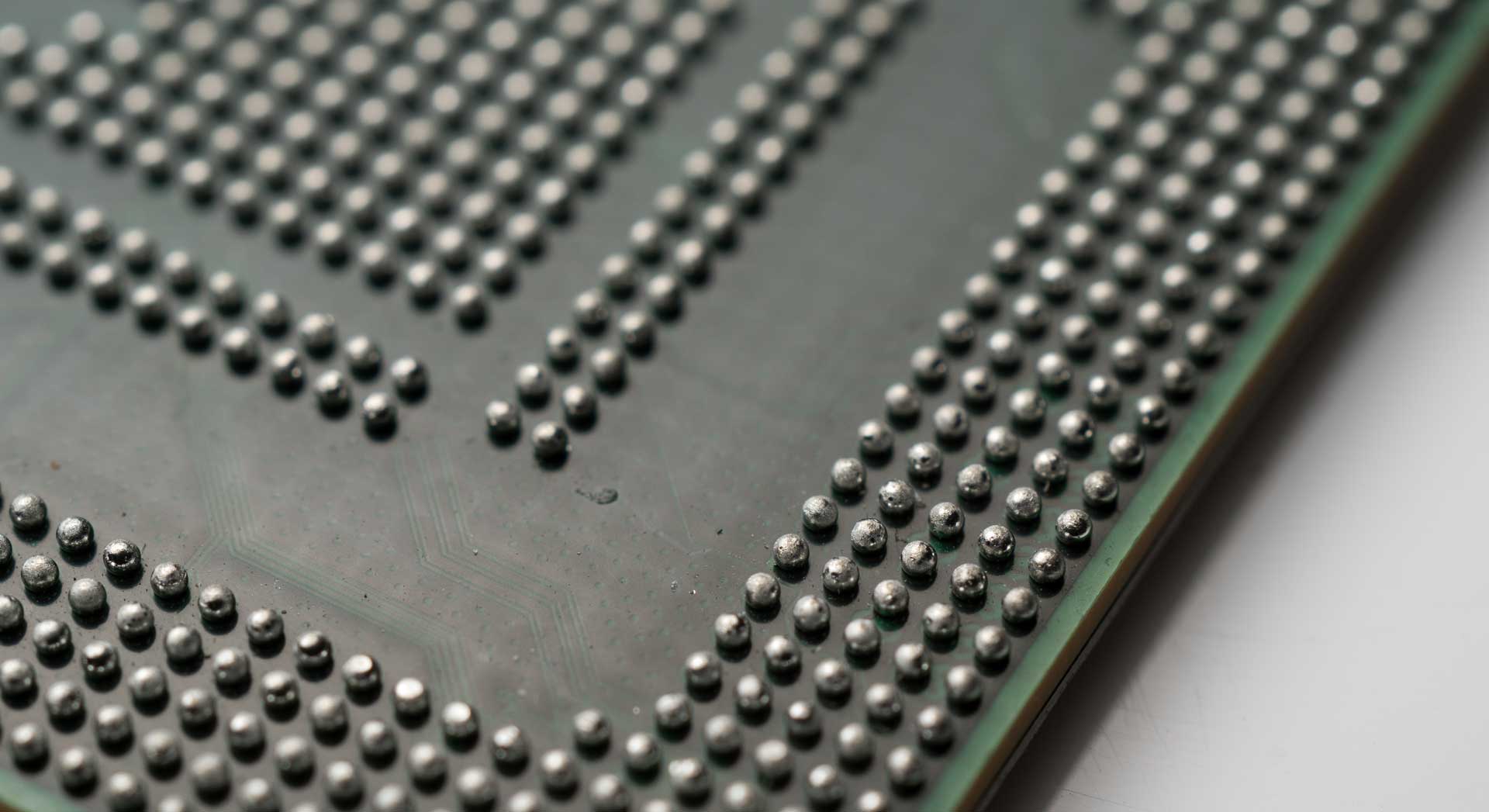
Viscom’s X-ray inspection detects hidden solder joint defects in BGA (Ball Grid Array) and QFN (Quad Flat No-Lead) Components, including voids, solder bridges, and head-in-pillow defects. Precise inspection of concealed connections enables early defect detection in complex SMT assemblies.
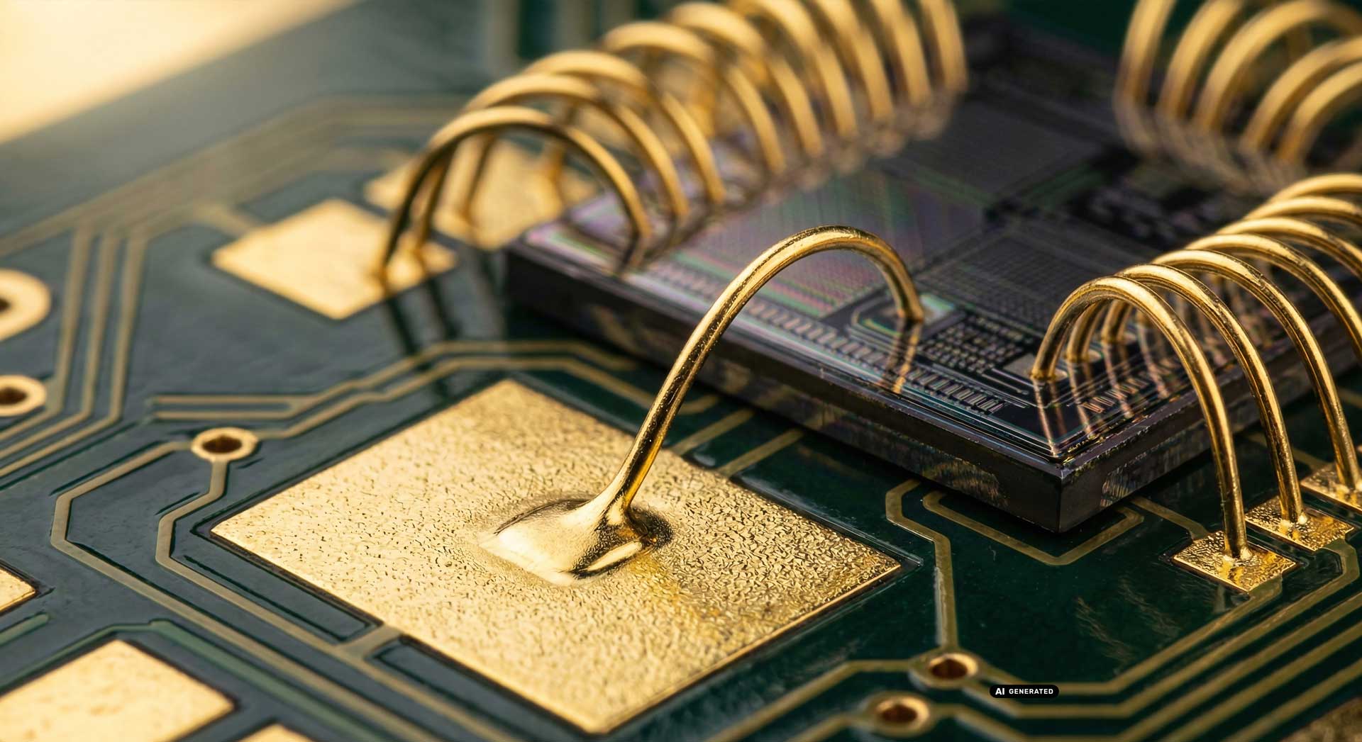
Wire Bond Inspection
As Wire Bonding moves toward thinner wires, finer pitches, and high-power applications, defect-free inspection becomes essential, especially in automotive and 5G Electronics.
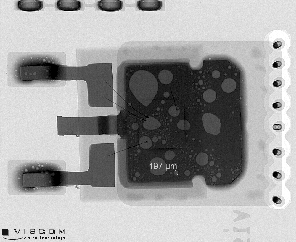
Void Inspection
Voids can develop within applications when air, gas, moisture, or contaminants become trapped during the application, dispensing, curing, or manufacturing process.