

Inline AOI Inspection System for Reliable Quality Control

iS6059 PCB Inspection Plus: Smartly networked with exceptional computing power and reliable measurement accuracy
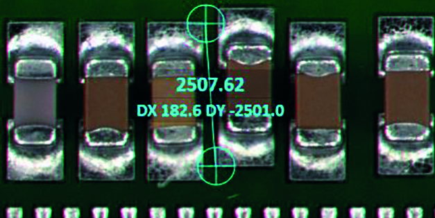
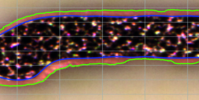
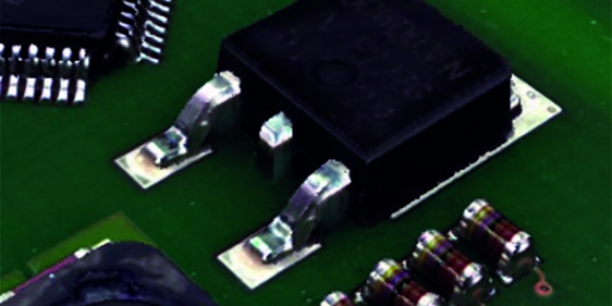
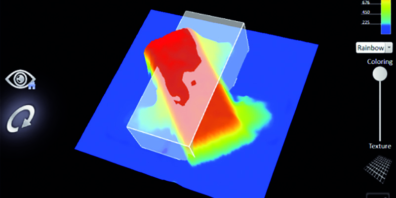
The iS6059 PCB Inspection Plus system rapidly checks that electronic components are in place, takes exact measurements of the heights on an assembly and inspects solder joints with high reliability. Nine views in first-class resolution and up to 26% more pixels, variable illumination, larger angled image fields with the same resolution, even further increased data transfer rates combined with 25% faster image capture and extensive networking options provide a solid basis for unbeatable line-integrated performance. Processes can be significantly improved and returns consistently avoided. Manufacturing costs can be trimmed in the long term and the high quality of even very sophisticated electronic products can be ensured.

Inspection scope
- Uncompromisingly good imaging thanks to state-of-the-art sensor technology
- High resolution for the precise inspection of microscopic components
- Large angled views for the most accurate analyses
- Smart verification with optional AI integration
- Intuitively simple operation and creation of inspection programs
- Fast data processing with powerful frame grabber
- Extremely fast handling of the inspection objects
- Expert service worldwide – online, by phone and on site
- Global libraries, global calibration: importability to all systems
- Traceability, offline programming, statistical process control
- Autonomous Viscom real-time image processing with analysis tools
- Simple process analysis with the Viscom Uplink Analyzer
| Components: up to 03015 and fine-pitch components |
| Solder joints, placement, open surfaces, character recognition, solder paste, configuration, assembly defects |
| Defects/defect features: excessive/insufficient solder, missing solder/solder skip, component missing, component offset, wrong component, component damaged, component overpopulated, billboarding, component on back, damaged pin, bent pin, solder bridging/short circuit, tombstoning, lifted lead, soldering defects, nonwetting, contamination, polarity error, rotation, imperfect shape |
| Optional: free area analysis, color ring analysis, wobble circle error, OCR, blow holes in the solder joint, solder ball/solder sputter |
| DIMENSIONS | |
| System housing: | 997 mm x 1756 mm x 1753 mm (39.2" x 69.1" x 69") (W x D x H) |
| CAMERA TECHNOLOGY | |
| 3D Camera technology: | XMplus-II |
| Z-resolution: | 0.5 μm |
| Field of view size: | 50 mm x 50 mm (1.9" x 1.9") |
| INSPECTION | |
| Speed: | Up to 80 cm²/s |
| HANDLING | |
| PCB dimensions: | 508 mm x 508 mm (20" x 20") |
| Longboard option available for circuit boards up to 720 mm (28,3") in length | |
| SOFTWARE | |
| User interface: | Viscom vVision/SI EasyPro |
ADVANTAGES AT A GLANCE
- Effective process optimization and avoidance of returns
- Latest 3D camera technology with XMplus-II sensor module
- High depth of field from every angle
- Variable illumination and larger angled fields of view at the same resolution
- Complete 360-degree views in 3D
- Higher data transfer rates with up to 25% faster image capture
- Exact height measurements of the smallest components
- Comprehensive networking options (vConnect, IPC/CFX, Hermes, and more)


